| Power System Blockset | |
Implement a gate turn-off (GTO) thyristor model.
Library
Description
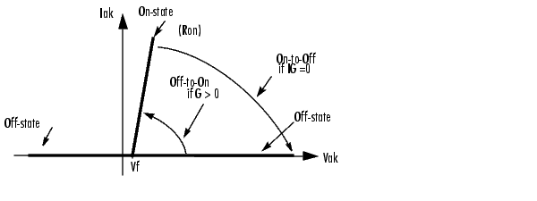
The Gate Turn-Off (GTO) thyristor is a semiconductor device that can be turned on and off via a gate signal. Like a conventional thyristor, the GTO thyristor can be turned on by a positive gate signal (g>0). However, unlike the thyristor which can be turned off only at a zero crossing of current, the GTO can be turned off at any time by applying a gate signal equal to zero.
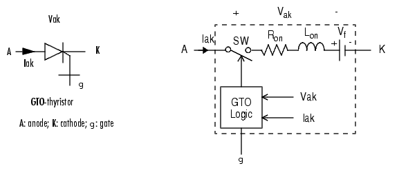
The GTO thyristor is simulated as a resistor (Ron), an inductor (Lon) and a DC voltage source (Vf) connected in series with a switch (SW). The switch is controlled by a logical signal depending on the voltage Vak, current Iak and the gate signal (g).
The GTO thyristor turns on when the anode-cathode voltage is greater than Vf and a positive pulse signal is present at the gate input (g>0). When the gate signal is set to zero, the GTO thyristor starts to block but its current does not stop instantaneously.
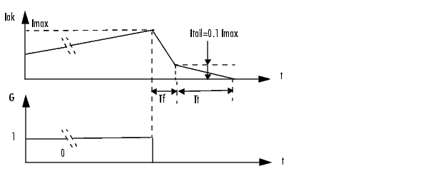
Since the current extinction process of a GTO thyristor contributes significantly to the turn-off losses, the turn-off characteristic is built into the model. The current decrease is approximated by two segments. When the gate signal becomes zero, the current Iak first decreases from the value Imax (value of Iak when the GTO thyristor starts to open) to Imax/10, during the fall time (Tf), and then from Imax/10 to zero during the tail time (Tt). The GTO thyristor turns off when the current Iak becomes zero. The latching and holding currents are not considered.
Vf, Ron, and Lon are the forward voltage drop while in conduction, the forward conducting resistance and the inductance of the device, respectively.
The GTO block contains a series Rs-Cs snubber circuit that can be connected in parallel with the GTO thyristor.
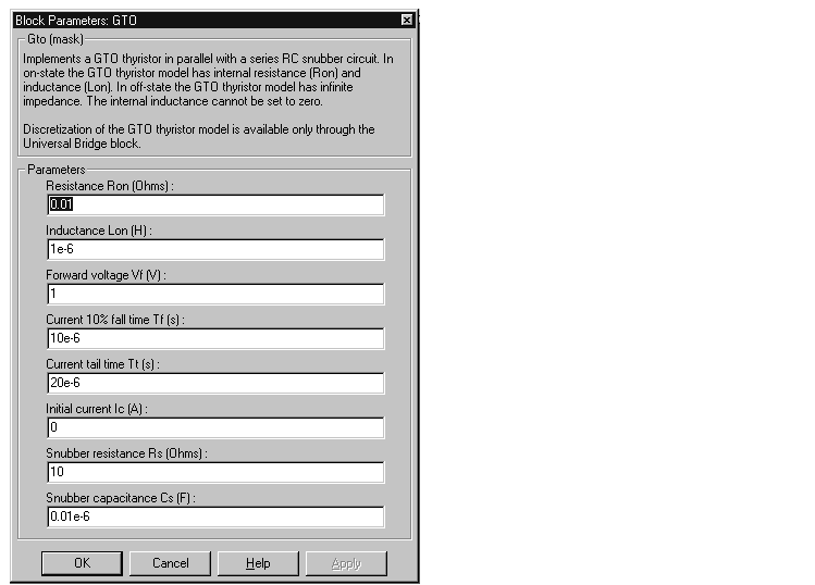
Dialog Box and Parameters
 ).
). 0.). Set the Snubber resistance Rs parameter to inf to eliminate the snubber from the model. 0 to eliminate the snubber, or to inf to get a purely resistive snubber.Inputs and Outputs
The first input and output are the GTO thyristor device terminals connected respectively to anode (a) and cathode (k). The second input (g) is a Simulink signal applied to the gate. The second output (m) is a Simulink measurement output vector [Iak, Vak] returning the GTO thyristor current and voltage.
Assumptions and Limitations
The GTO block implements a macro-model of a real GTO thyristor. It does not take into account either the geometry of the device or the underlying physical processes of the device [1].
The GTO block requires a continuous application of the gate signal (g>0) in order to be in the on-state (with Iak>0). The latching current and the holding current are not considered. The critical value of the derivative of the re-applied anode-cathode voltage is not considered.
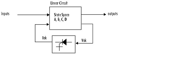
The GTO block is modeled as a nonlinear element interfaced with the linear circuit, as shownon the next figure.
Therefore, in order to avoid an algebraic loop, the GTO block inductance Lon cannot be set to zero. Each GTO block adds an extra state to the electrical circuit model. The GTO block is modeled as a current source. It cannot be connected in series with an inductor, a current source, or an open circuit, unless its snubber circuit is used.
Circuits containing individual GTO blocks cannot be discretized. However discretization is permitted for GTO/Diodes bridges simulated with the Universal Bridge block.
You must use a stiff integrator algorithm to simulate circuits containing GTO blocks. Ode23tb or Ode15s with default parameters usually give best simulation speed.
Example
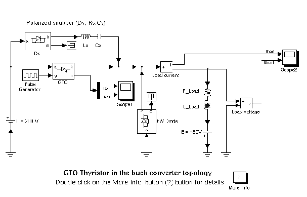
The following example illustrates the use of the GTO block in a buck converter topology. The basic polarized snubber circuit is connected across the GTO block. The snubber circuit consists of a capacitor Cs, a resistor Rs and a diode Ds. The parasitic inductance Ls of the snubber circuit is also taken into consideration.
The parameters of the GTO block are those found in the Dialog Box section, except for the internal snubber which is out of service (Rs=Inf Cs=0).
The switching frequency is 1000 Hz and the pulse width is 216 degrees (duty cycle 60%). This example is available in the psbbuckconv.mdl file.
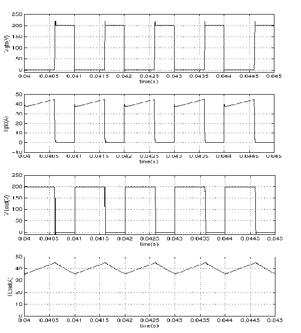
Run the simulation. Observe the GTO block voltage and current as well as, the load voltage and current.
References
[1] Mohan N., Power Electronic, Converters, Applications and Design, John Wiley & Sons, Inc., New York, 1995
See Also
Diode, Thyristor, Mosfet, Ideal Switch
| | Ground | Hydraulic Turbine and Governor | |