| Power System Blockset | |
Implement an ideal switch device.
Library
Description
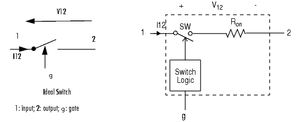
The Ideal Switch block does not correspond to a particular physical device. When used with appropriate switching logic, it can be used to model simplified semiconductor devices such as a GTO or a MOSFET, or even a power circuit breaker with current chopping. The switch is simulated as a resistor (Ron) in series with a switch controlled by a logical g.
The Ideal Switch block also contains a series Rs-Cs snubber circuit that can be connected in parallel with the ideal switch.
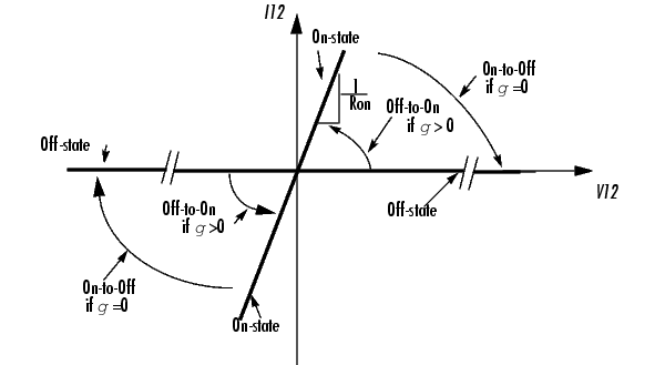
The Ideal Switch block is fully controlled by the gate signal (g>0 or g=0). It has the following characteristics:
The Ideal Switch block turns on when a positive signal is present at the gate input (g>0). It turns off when the gate signal equals zero (g=0).
Dialog Box and Parameters
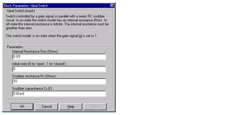
 ). The Internal resistance Ron parameter cannot be set to zero.
1 (closed) the states of the linear circuit are automatically initialized so that the simulation starts in steady state.). Set the Snubber resistance Rs parameter to inf to eliminate the snubber from the model. 0 to eliminate the snubber, or to inf to get a purely resistive snubber.Inputs and Outputs
The first input (1) and output (2) of the block are the ideal switch electrical connections. The second input (g) is a Simulink signal applied to the gate. The second output (m) is a Simulink measurement output vector [Iak,Vak] returning the Ideal Switch block current and voltage.
Assumptions and Limitations
The Ideal Switch block is modeled as a current source, therefore it cannot be connected in series with an inductor, a current source or an open circuit, unless a snubber circuit is used.
You must use a stiff integrator algorithm to simulate circuits containing Ideal Switch blocks. Ode23tb or Ode15s with default parameters usually give best simulation speed.
Example
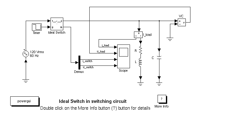
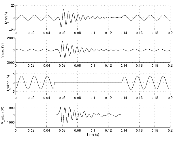
An Ideal Switch block is used to switch an RLC circuit on an AC source (60 Hz). The switch, which is initially closed, is first open at t=50 ms (3 cycles) and then reclosed at t=138 ms (8.25 cycles).The Ideal Switch block has a 0.01 ohms resistance and no snubber is used. This example is available in the psbswitch.mdl file.
Run the simulation and observe the inductor current, the switch current and the capacitor voltage. Notice the high frequency overvoltage produced by inductive current chopping. Note also the high switch current spike when the switch is reclosed on the capacitor at maximum source voltage.
See Also
References
Mohan, N., Power Electronic, Converters, Applications and Design, John Wiley & Sons, Inc., New York, 1995.
| | Hydraulic Turbine and Governor | IGBT | |