| Power System Blockset | |
Library
Description
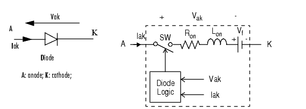
A diode is a semiconductor device that is controlled by its own voltage and current. When a diode is forward biased (Vak>0), it starts to conduct with a small forward voltage across it. It turns off when the current flow into the device becomes zero. When the diode is reverse biased (Vak<0), it stays in the off-state.
The Diode block is simulated as a resistor, an inductor, and a DC voltage source (Vf) connected in series with a switch. The switch is controlled by the voltage Vak and current Iak.
The Diode block also contains a series Rs-Cs snubber circuit that can be connected in parallel with the diode device.
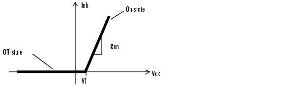
The static VI characteristic of this model is shown in the figure below.
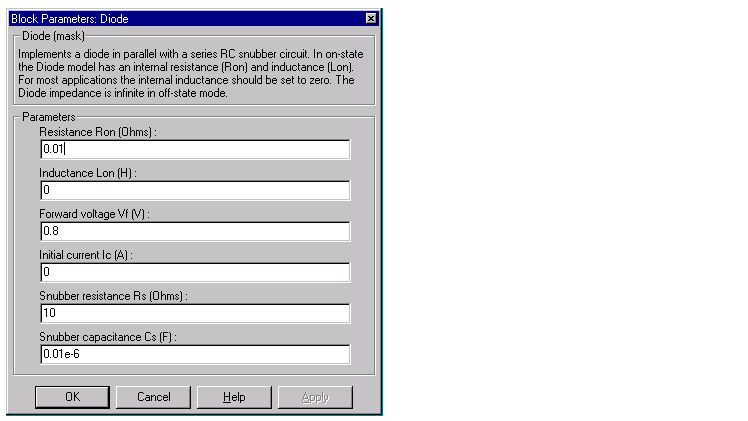
Dialog Box and Parameters
 ). The Resistance Ron parameter cannot be set to
 0 when the Inductance Lon parameter is set to 0.0 when the Resistance Ron parameter is set to 0.). Set the Snubber resistance Rs parameter to inf to eliminate the snubber from the model. 0 to eliminate the snubber, or to inf to get a purely resistive snubber.Inputs and Outputs
The input of the block is the anode (a) of the diode and the first output is the cathode (k). The second output (m) is a Simulink measurement output vector [Iak, Vak] returning the diode current and voltage.
Assumptions and Limitations
The Diode block implements a macro-model of a diode device. It does not take into account either the geometry of the device or the complex physical processes underlying the state change [1]. The leakage current in the blocking state and the reverse-recovery (negative) current are not considered. In most circuits, the reverse current does not affect converter or other device characteristics.
Depending on the value of the inductance Lon, the diode is modeled either as a current source (Lon>0) or as a variable topology circuit (Lon=0). See Advanced Topics chapter for more details on this topic.
As the diode device is modeled as a current source, the Diode block cannot be connected in series with an inductor, a current source, or an open circuit, unless its snubber circuit is in use.
You must use a stiff integrator algorithm to simulate circuits containing diodes. Ode23tb or Ode15s with default parameters usually give best simulation speed.
The inductance Lon will be forced to zero if you choose to discretize your circuit.
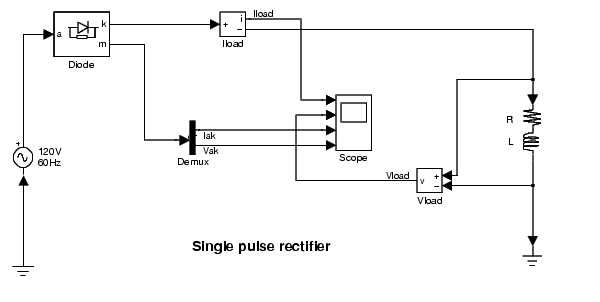
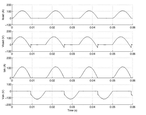
Example
Single pulse rectifier consisting of a Diode block, an RL load, and an AC Voltage source block, with the following parameters:
Diode block: Ron = 0.001 , Lon = 0 H, Vf = 0.8 V, Rs= 20 , Cs= 4e-6
F; R=1 L=1mH.
This circuit is available in the psbdiode.mdl file. Simulation produces the following results:
References
[1] Rajagopalan, V., Computer-Aided Analysis of Power Electronic Systems, Marcel Dekker, Inc., New York,1987.
[2] Mohan, N., Power Electronic, Converters, Applications and Design, John Wiley & Sons, Inc., New York, 1995.
See Also
Thyristor, Universal Bridge
| | DC Voltage Source | Discrete System | |