| Power System Blockset | |
Implement an Insulated-Gate-Bipolar-Transistor (IGBT).
Library
Description
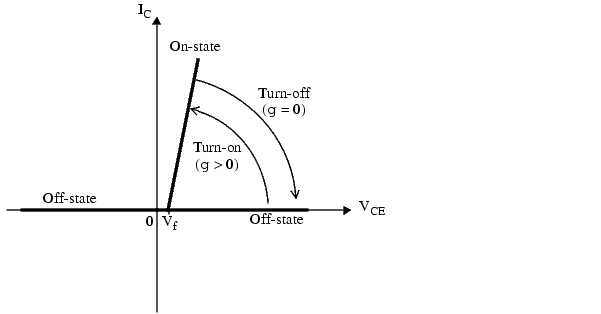
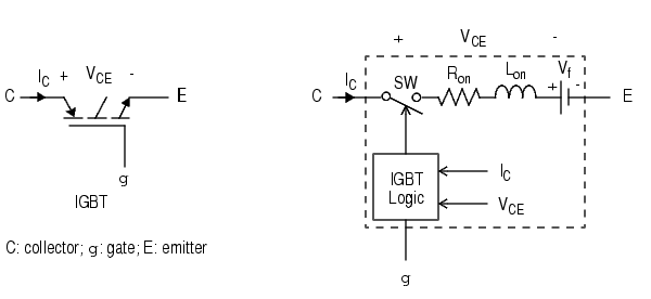
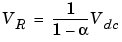
The IGBT block implements a semiconductor device controllable by the gate signal. The IGBT is simulated as a series combination of a resistor (Ron), and inductor (Lon), and a DC voltage source (Vf) in series with a switch controlled by a logical signal (g>0 or g=0).
The IGBT turns on when the collector-emitter voltage is positive and greater than Vf and a positive signal is applied at the gate input (g > 0). It turns off when the collector-emitter voltage is positive and a zero signal is applied at the gate input (g = 0).
The IGBT device is in off-state when the collector-emitter voltage is negative. Note that many commercial IGBTs do not have the reverse blocking capability. Therefore, they are usually used with an anti-parallel diode.
The IGBT block contains a series Rs-Cs snubber circuit, which is connected in parallel with the IGBT device.
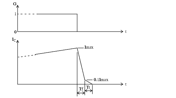
The turn-off characteristic of the IGBT model is approximated by two segments. When the gate signal falls to zero, the collector current will decrease from Imax to 0.1Imax during the fall time (Tf), and then from 0.1Imax to zero during the tail time (Tt).
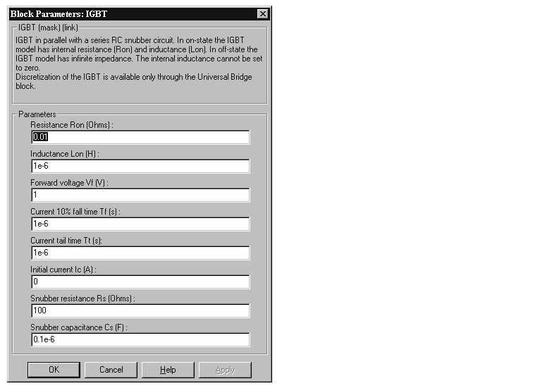
Dialog Box and Parameters
 ).
). 0 ). Set the Snubber resistance Rs parameter to inf to eliminate the snubber from the model. 0 to eliminate the snubber, or to inf to get a purely resistive snubber.Inputs and Outputs
The first input and output are the IGBT terminals connected respectively to collector (c) and emitter (e). The second input (g) is a logical Simulink signal applied to the gate. The second output is a Simulink measurement vector [Ic, Vce] returning the IGBT current and voltage.
Assumptions and Limitations
The IGBT block implements a macro-model of the real IGBT device. It does not take into account either the geometry of the device or the complex physical processes [1].
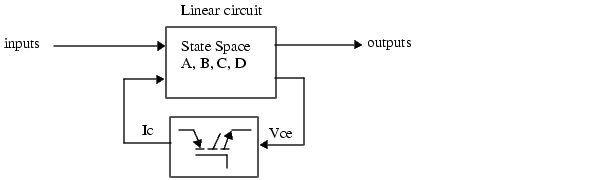
The IGBT is modeled as a nonlinear element interfaced with the linear circuit as shown below.
Therefore, in order to avoid an algebraic loop, the IGBT inductance Lon cannot be set to zero. Each IGBT adds an extra state to the electrical circuit model. As the IGBT is modeled as a current source, it cannot be connected in series with an inductor, a current source, or an open circuit, unless a snubber circuit is used.
Circuits containing individual IGBT blocks cannot be discretized. However discretization is permitted for IGBT/Diodes bridges simulated with the Universal Bridge block.
You must use a stiff integrator algorithm to simulate circuits containing IGBTs. Ode23tb or Ode15s with default parameters usually give best simulation speed.
Example
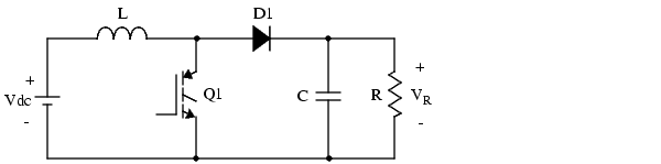
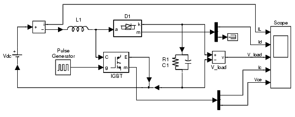
The following example illustrates the use of the IGBT block in a boost dc-dc converter. The IGBT is switched on and off at a frequency of 10 kHz to transfer energy from the DC source to the load (RC). The average output voltage (VR) is a function of the duty cycle ( ) of the IGBT switch:
This example is available in the psbigbtconv.mdl file.
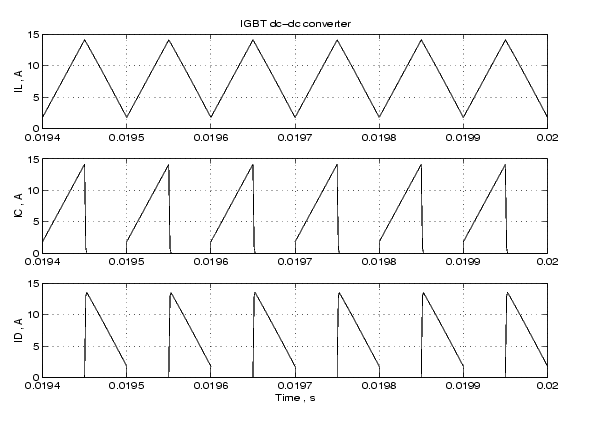
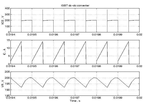
Run the simulation and observe the inductor current (IL), the IGBT collector current (IC), the diode current (ID), the IGBT device collector-emitter voltage (VCE), and the load voltage (VR).
References
[1] Mohan, N., Power Electronic, Converters, Applications and Design. John Wiley & Sons, Inc., New York, 1995.
See Also
GTO, Thyristor, MOSFET, Universal Bridge
| | Ideal Switch | Impedance Measurement | |